M.2 Evaluation Device - Bottom Pad Version🔗
Introduction🔗
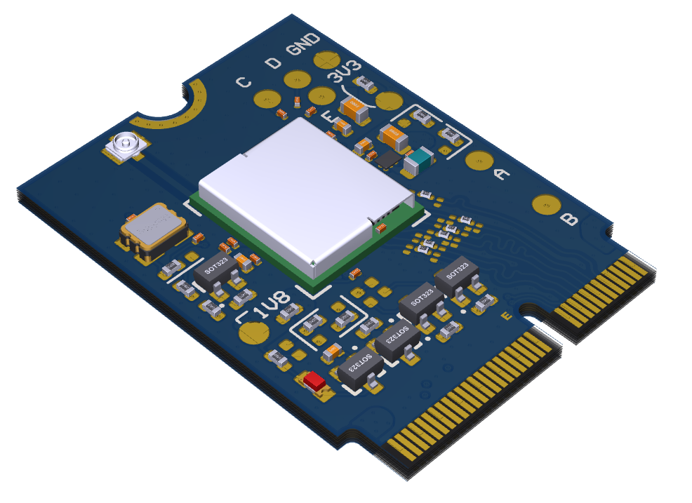
The PAN W602-2B M.2 device is an Evaluation Device (EVD) that is designed for evaluating the PAN W602-2B module in conjunction with host processor evaluation kits that have a M.2 Key E socket.
There is no dedicated M.2 evaluation device for the single-band PAN W602-1B module. However, the M.2 evaluation device can also be used for PAN W602-1B evaluation. To ensure representative results, operation shall be limited to the feature set supported by the PAN W602-1B, and functions exclusively available in the PAN W602-2B shall not be used.
Schematics for the M.2 card are available in the Downloads section.
Features🔗
- M.2 Key E connector
- SWD Interface (via Test Points)
- MHF® 4L connector for optional conducted RF testing
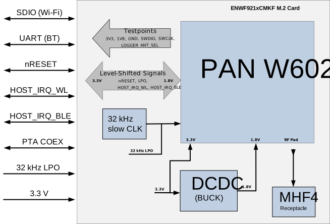
- On-board DC/DC converter (3.3 V to 1.8 V)
- 32 kHz oscillator for low power evaluation
- Configurable routing options for nRESET and WLAN interrupt signals
- Multiple test points for measurement and debugging
Block Diagram🔗
Board Overview🔗
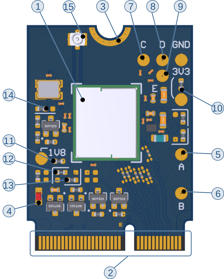
1
The Module
PAN W602-2B wireless communication module mounted on the evaluation device.
2
M.2 Key E connector
Standard M.2 Key E edge connector that interfaces the module with a compatible host processor platform. For pin assignment details, refer to M.2 Connector Pin Map
3
Mounting Screw Hole
Mechanical mounting point used to secure the device in an M.2 Key E socket. For mounting instructions, refer to Mounting the Device
4
Status LED
Visual indicator that provides information about the current operating status and activity of the device.
5
Test Point - A
GPIO1 - Provides access to the GPIO1 signal, which can be used for antenna selection and validation during development.
6
Test Point - B
LOGGER - Provides access to the UART logging interface, enabling debugging and runtime diagnostics during development.
7
Test Point - C
SWDIO -Serial Wire Debug data signal used for device programming and debugging.
8
Test Point - D
SWDCLK - Serial Wire Debug clock signal used together with SWDIO for device programming and debugging.
9
Test Point - E
nRESET - Active-low reset signal that allows the module to be reset during development, debugging, and testing.
10
Power Option 3V3 - R1
Test point and configuration area for supplying or monitoring the 3.3 V power rail used by the module.
11
Power Option 1V8 - R2
Test point and configuration area for supplying or monitoring the 1.8 V power rail used by the module.
12
nRESET Jumper
Configuration jumper used to select the M.2 Key E pin connected to the module reset signal.
13
HOST_IRQ_BLE Jumper
Configuration jumper used to select the M.2 Key E pin assignment for the Bluetooth host interrupt signal.
14
Slow-Clock Jumper
Selects whether the module uses the internal clock source or an external 32 kHz reference clock.
15
MHF 4L Module Connector - X1
MHF 4L connector directly connected to the module RF port, allowing connection of external antennas or RF test equipment.
Initial Preparations🔗
Mounting the Device🔗
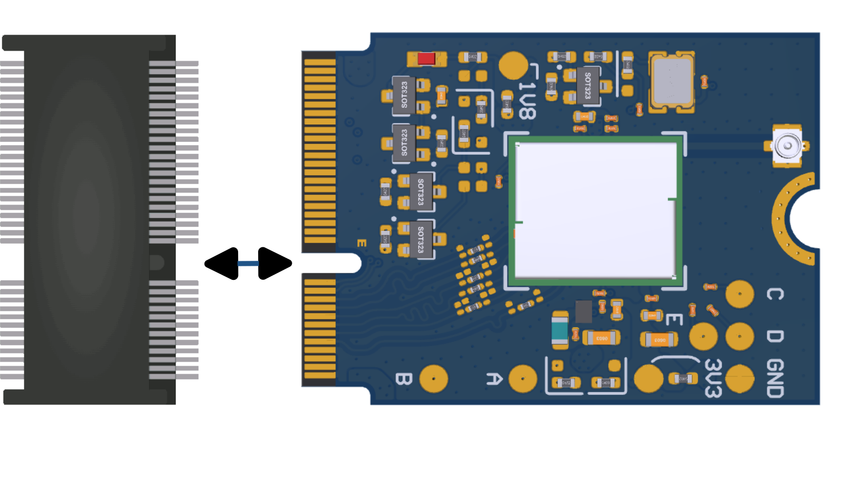
To mount the PAN W602-2B M.2 device in a M.2 Key E socket on a host board execute the following instructions.
-
Line up the notch on the M.2 Key E connector 2 with the key of the M.2 Key E socket of the host board.
-
Insert the PAN W602-2B M.2 device into the socket at a slight angle.

-
Apply light downward pressure until the PAN W602-2B M.2 device is parallel to the host board and makes contact with the threaded insert.

-
Insert an M2.5 x 4 machine screw into the mounting Screw Hole 3 and the threaded insert.

The PAN W602-2B M.2 device is secured in place.
M.2 Connector Pin Map🔗
| Description | M.2 Key E Pin | Function | Module Footprint | Module Pin |
|---|---|---|---|---|
| SDIO Interface | 9 | SDIO Clock | A2 | SDIO_CLK |
| 11 | SDIO Command | A1 | SDIO_CMD | |
| 13 | SDIO data line 0 | A25 | SDIO_D0 | |
| 15 | SDIO data line 1 | B1 | SDIO_D1 | |
| 17 | SDIO data line 2 | A24 | SDIO_D2 | |
| 19 | SDIO data line 3 | B13 | SDIO_D3 | |
| UART Interface | 22 | UART receive | B12 | UART_RX |
| 32 | UART transmit | A22 | UART_TX | |
| 36 | UART ready-to-send | B11 | UART_RTS | |
| 34 | UART clear-to-send | A21 | UART_CTS | |
| Reset Signals | 23 | Reset input | B81 | nRESET1 |
| 56 | Reset input | B82 | nRESET2 | |
| Wake Signals | 21 | Interrupt request for Wi-Fi / Host wakeup | A53 | HOST_IRQ_WL3 |
| 62 | Interrupt request for Wi-Fi / Host wakeup | A54 | HOST_IRQ_WL4 | |
| 20 | Interrupt request for Bluetooth / Host wakeup | B45 | HOST_IRQ_BLE5 | |
| Coexistence Interface |
44 | Packet traffic arbitration (coexistence) priority signal | A19 | COEX_PRI |
| 46 | Packet traffic arbitration (coexistence) grant signal | A18 | COEX_GRA | |
| 48 | Packet traffic arbitration (coexistence) request signal | B10 | COEX_REQ | |
| Power | 2, 4, 72, 74 | 3.3 V | A6, B5 | 3V3 |
| 1, 7, 18, 33, 39, 45, 51, 57, 63, 69, 75 | GND | A7, A8, A9, A10, A11, A12, A14, A15, A23, B2, B6, B7, B9 | GND |
Some of the M.2 Key E pins are not directly connected to the PAN W602-2B. Whether these pins are functional depends on the assembly options configured on the PAN W602-2B M.2 device. You have to check the schematics and your device configuration carefully.

Jumper Overview🔗
| Signal | Additional Information |
|---|---|
| nRESET | Hardware reset input to restart the module |
| HOST_IRQ_BLE | Interrupt line used by module to signal the host |
| Slow Clock | 32 kHz clock input used for low-power timing |
nRESET🔗
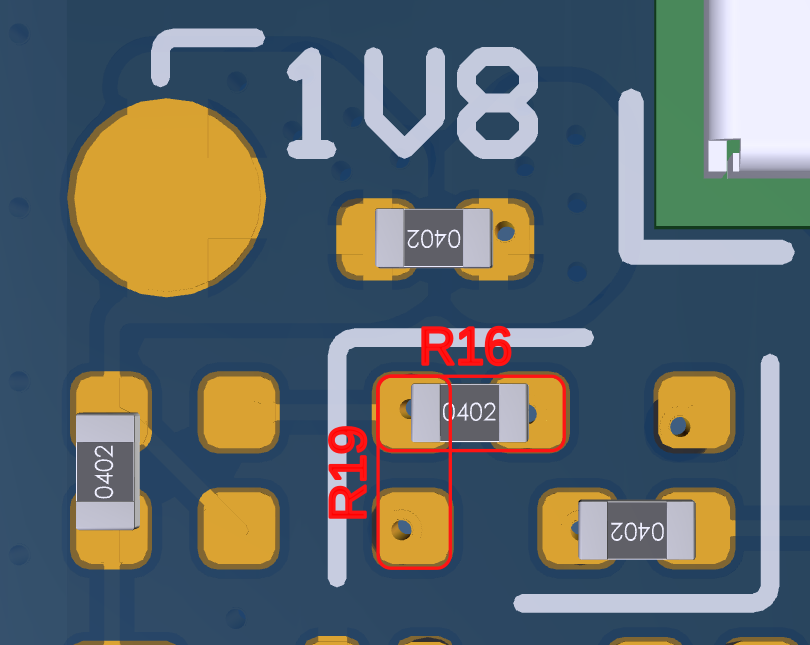
| R16 | R19 | Description |
|---|---|---|
| 0 Ω | DNP | Uses the first M.2 Key-E pin assignment option (Pin 56) for nRESET |
| DNP | 0 Ω | Uses the second M.2 Key-E pin assignment option (Pin 23) for nRESET |
HOST_IRQ_BLE🔗
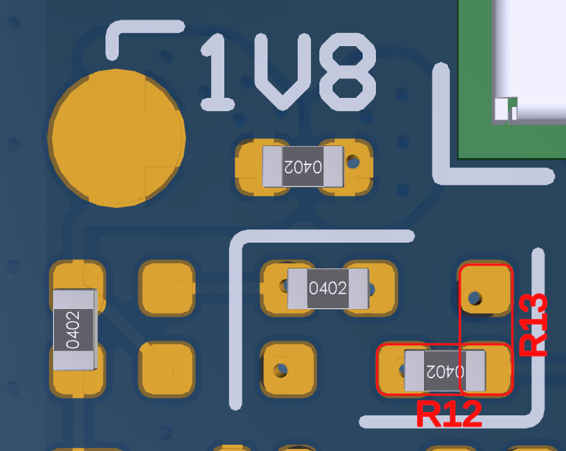
| R12 | R13 | Description |
|---|---|---|
| 0 Ω | DNP | Uses the first M.2 Key-E pin assignment option (Pin 21) for HOST_IRQ_BLE |
| DNP | 0 Ω | Uses the second M.2 Key-E pin assignment option (Pin 62) for HOST_IRQ_BLE |
Slow Clock🔗
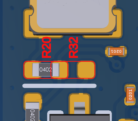
| R20 | R32 | Description |
|---|---|---|
| 0 Ω | DNP | Usage of an internal 32 kHz slow clock (M.2 Key-E Card) |
| DNP | 0 Ω | Usage of an external 32 kHz slow clock (Host Platform) |
Test Points Overview🔗
| Test Point | Description | Additional Information |
|---|---|---|
| A | GPIO1 (ANT_SEL) | GPIO signal used for antenna selection |
| B | LOGGER | Debug and logging output signal |
| C | SWDIO | Serial Wire Debug data signal |
| D | SWDCLK | Serial Wire Debug clock signal |
| E | nRESET | Active-low reset signal |
| GND | GND | Ground reference |
Test Point A - GPIO1 (ANT_SEL)🔗
The ANT_SEL signal available at test point A 5 can be manually controlled by the Linux host to change its logic level. After power‑up, the pin is LOW by default. Specific commands allow setting it to HIGH (1) or LOW (0).
Test Point B - LOGGER🔗
The module provides a dedicated LOGGER test point B 9 that exposes the device’s UART‑TX debug output. This interface allows direct access to the system’s diagnostic logger stream for development and troubleshooting purposes.
Test Points C,D,E - SWD Interface🔗
The module can be accessed directly through its SWD interface. The mentioned test points can be used to connect an LP‑XDS110 debug probe. This setup enables external tools, such as the Radio Tool included in the SimpleLink Wi‑Fi Toolbox, to communicate directly with the module without requiring a host processor.
Power Options🔗
| Voltage | Jumper | Description |
|---|---|---|
| 1V8 | R2 | Possibility to power the module independent from host board |
| 3V3 | R1 | Possibility to power the module independent from host board, bypassing the on-board DC/DC converter if required. |
When the PAN W602-2B M.2 device shall be supplied externally while it’s still inserted in a host board (for example for current measurements), then please remove the two chip jumpers 11 and 10.
-
This pin controls the nReset_op2 signal on your PAN W602-2B M.2 device (Not connected by default). ↩↩
-
This pin controls the nReset_op1 signal on your PAN W602-2B M.2 device (Connected by default). ↩↩
-
This pin controls the toHost_nIRQ_WL_op1 signal on your PAN W602-2B M.2 device (Connected by default). ↩↩
-
This pin controls the toHost_nIRQ_WL_op2 signal on your PAN W602-2B M.2 device (Not connected by default). ↩↩
-
According to this TI E2E forum discussion post the host wake up functionality for Bluetooth is not supported yet. ↩↩