User Guide🔗

The revision 2 of the PAN1780 evaluation board (ENW89854AUKF) features the same PAN1780 Bluetooth® Low Energy (LE) module (ENW89854A1KF) which is based on the Nordic Semiconductor nRF52840 single-chip controller.

The revision 2 of the PAN1770 evaluation board (ENW89854CXKF) features the same PAN1770 Bluetooth® Low Energy (LE) module (ENW89854A1KF) which is based on the Nordic Semiconductor nRF52840 single-chip controller.
A PULSE W1030 antenna and a micro coax cable are included.
Introduction🔗
You can access all the different module interfaces like USB, UART, GPIOs, current measurement pins, and Segger J-Link on-board debugger easily, which makes the evaluation board ideally suited for the evaluation of the module and rapid prototyping of products.
Warning
During development, module-specific information, which also includes the Bluetooth Device Address, may get lost. Before you start any development, it is recommended to save module-specific information.
Please refer to Bluetooth Device Address Safeguard.
Changes🔗
These are the things that changed in comparison to revision 1 of the evaluation board:
- The separate FTDI USB to UART device was removed. Now you can use the built-in UART functionality of the Segger J-Link on-board debugger instead.
- Because of this, the USB hub was removed as well, because it was no longer needed.
- The dedicated pins for the Segger J-Link on-board debugger and the Auxillary UART connection pin header were also removed.
You won't notice any functional changes when using the revision 2 of the evaluation board instead of revision 1.
Features🔗
- Arduino interface configurable as shield or board
- All GPIOs accessible via pin headers
- Power measurement interface
- Segger J-Link on-board debugger
- Peripherals can be deactivated for low power applications
- 4x user buttons, 4x user LEDs
- Module native USB interface
- NFC antenna connector
- Compatible to nRF Connect SDK projects
Block Diagram🔗

Board Overview🔗

1
USB connector - X1
You can use the USB connector to power the board and gain access to the UART communication and debugging capabilities. Also see Powering Options
2
Reset button
You can use the reset button to reset the board to a known-good state.
3
User buttons
You can use the user buttons to interact with the running application if the application supports it.
4
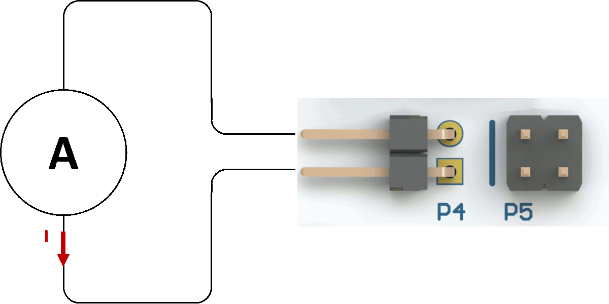
Current measurement pin header - P4
You can use the current measurement pin header to measure the current consumption of the currently running application. Also see Powering OptionsCurrent Consumption Measurement
5
Module power supply pin header - P5
You can use the module power supply pin header to disconnect the power to the module for current consumption measurement purposes. Also see Current Consumption Measurement
6
Module native USB connector - X5
You can use the module native USB connector to interact with the USB interface of the module. It is directly connected to module's USB pins. Also see Powering Options
7
UART module connection pin header - P1
You can use the UART module connection pin header to interact with the USB serial device or the default UART pins that are usually used. The UART pins are directly connected to the module. You can cut the connection here in order to isolate the module for Current Consumption Measurement.
8
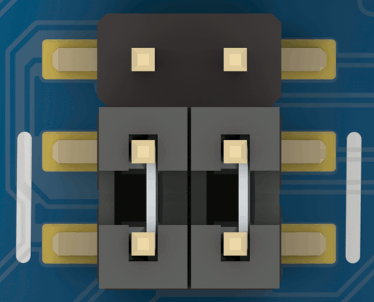
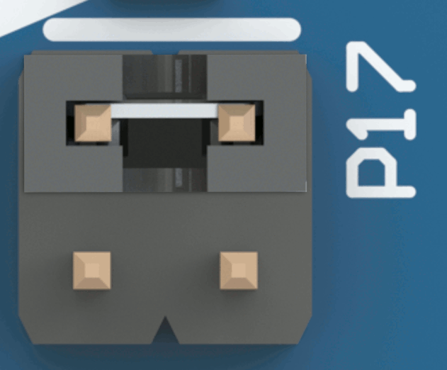
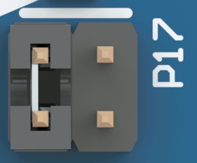
Arduino power direction pin header - P17
You can use the Arduino power direction pin header to configure the operation when using the Arduino pin headers. Also see Arduino Configuration
9
User LEDs
You can use the user LEDs from the application to interact with the user.
10
Arduino pin headers - P9, P10, P11, P13
You can use Arduino pin headers to attach to Arduino shields or boards. Also see Arduino Interface
11
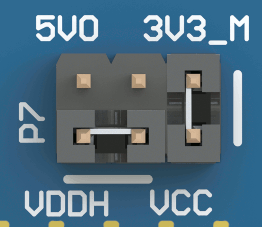
Power configuration pin header - P7
You can use power configuration pin headers to choose between 3.3 V and 5 V voltage levels. Also see Module Power Options
12
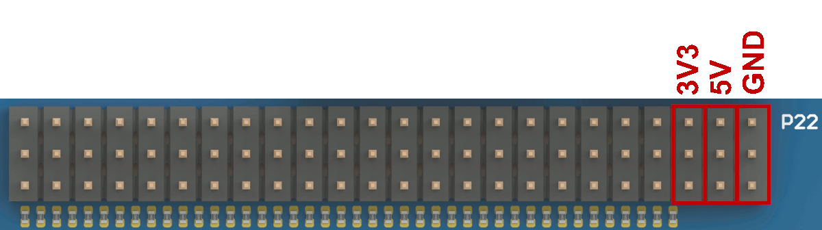
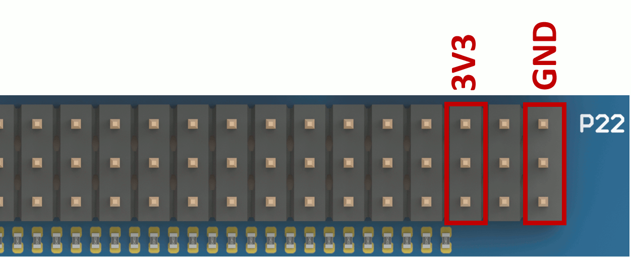
Breakout pin headers - P21 and P22
You can use the breakout pin headers to access all the module GPIO pins directly. Also see GPIO Pin Access
13
Power LED
You can observe the power LED to verify that the board is correctly powered.
14
The module
15
NFC antenna connector - P19
You can use the NFC antenna connector to connect an NFC antenna.
16
NFC pin header - P23
You can use the NFC pin header to access the NFC pins directly.
17
User LED pin header - P20
You can use the user LED pin header to control the connection of the LEDs to the module pins.
18
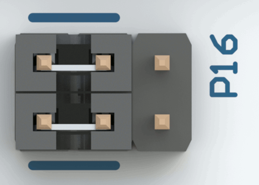
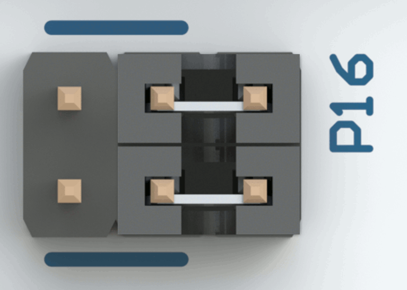
Arduino UART direction pin header - P16
You can use the Arduino UART direction pin headers to choose the configuration when running in shield or board mode. Also see Arduino Configuration
21
Segger J-Link LED
You can use the Segger J-Link LED to verify that the Segger J-Link on-board debugger is correctly powered.
23
Peripheral disable pin header - P6
You can use the peripheral disable pin header to control the connection of the peripherals like the Segger J-Link on-board debugger to the power supply. This is useful to disconnect certain peripherals for current consumption measurements.
24
Power pins on Arduino pin header - P11
You can use these power pins on the Arduino pin header to power the board. Also see Powering Options
25
Power pins on breakout pin header - P22
You can use these power pins on the breakout pin header to power the board. Also see Powering Options
Initial Preparations🔗
Before you can work with the evaluation tool (again) you may have to check (or restore) the default jumper configuration or install device drivers, depending on the operating system you are using.
Default Jumper Configuration🔗
You can check the default jumper configuration easily because it is imprinted with white (or blue) line markings on the silkscreen of the PCB.
For example, the default jumper configuration in the following picture is:
- One jumper put on the lower left two pins
- One jumper put on the lower right two pins
Segger J-Link On-Board Debugger Driver🔗
When you install one of the Development Tools from Nordic Semiconductor a driver for the Segger J-Link on-board debugger is automatically installed as well.
First Steps🔗
You can use a micro USB cable to connect the evaluation board to your computer using the USB connector X1 1.
The PAN1780 module is pre-programmed with a test application that is used during the production of the evaluation board.
You can observe the following behavior of the evaluation board after the very first start:
- The LEDs blink periodically.
- Logging is redirected to the real time transfer (RTT) interface, you can observe it with a suitable RTT Viewer, like the one integrated in the nRF Connect for VS Code extension.
- If you touch the NFC antenna with an NFC-capable reader device like a mobile phone, then the tag information is read which contains a link to the Wireless Connectivity at Panasonic Industry website.
- Because code from the Bluetooth: Peripheral UART is integrated, you can connect via Bluetooth and exchange information using the Nordic UART Service (NUS).
- If you press the button and you are observing the Nordic UART Service output using a mobile app, then you can see that some text is sent.
You can now start to set up a software development environment and then build and run your own application, check out the dedicated Getting Started guide.
Warning
During development, module-specific information, which also includes the Bluetooth Device Address, may get lost.
So before you start right now, it is recommended to save module-specific information first.
Please refer to Bluetooth Device Address Safeguard.
Pin Map🔗
| Header | Item | Function | Module Footprint | Module Pin | nRF52840 Footprint | nRF52840 Pin |
|---|---|---|---|---|---|---|
| P1 | 7 | UART Rx | C1 | P0.06 | E9 | P0.06 |
| UART Tx | B1 | P0.08 | E10 | P0.08 | ||
| UART CTS | D3 | P0.07 | F9 | P0.07 | ||
| UART RTS | A4 | P0.05 | D10 | P0.05 | ||
| P4 | 4 | Current Consumption Measurement | ||||
| P5 | 5 | Current Consumption Measurement | ||||
| P6 | 23 | Peripheral Configuration | ||||
| P7 | 11 | Powering Options | ||||
| P9, P10, P11, P13 | 10 | Arduino Interface | ||||
| P16 | 18 | RX/TX Direction | D7 | P1.02 | G3 | P1.02 |
| RX/TX Direction | F7 | P1.01 | J1 | P1.01 | ||
| P17 | 8 | Arduino Configuration | ||||
| P20 | 17 | LED1 | F3 | P0.13 | H7 | P0.13 |
| LED2 | F4 | P0.14 | J7 | P0.14 | ||
| LED3 | F5 | P0.15 | K7 | P0.15 | ||
| LED4 | G1 | P0.16 | H6 | P0.16 | ||
| P21 and P22 | 12 | GPIO Pin Access | ||||
| P23 | 16 | NFC1 | A9 | P0.09 | F1 | P0.09 |
| NFC2 | A8 | P0.10 | E2 | P0.10 | ||
Powering Options🔗
You can power the evaluation board in different ways:
- USB connector X1 1
- module native USB connector X5 6
- current measurement pin header P4 4
- power pins on Arduino pin header P11 24
- power pins on breakout pin header P22 25
Risk of damaging board components
Do not supply 5 V on the 3.3 V pin of the power pins on Arduino pin header P11 24 or the power pins on breakout pin header P22 25.
USB Connector🔗
You can power the whole evaluation board using the USB connector X1 1.
Note
Please note that the module is still powered if the peripherals are deactivated using peripheral disable pin header P6 23.
Module Native USB Connector🔗
You can power the whole evaluation board using the module native USB connector X5 6.
Note
Please note that the module is still powered if the peripherals are deactivated using peripheral disable pin header P6 23.
Current Measurement Pin Header🔗
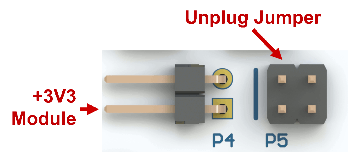
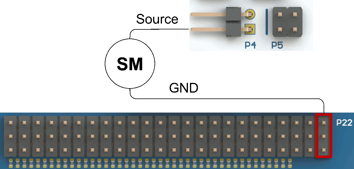
You can power the module by attaching VCC to the current measurement pin header P4 4.
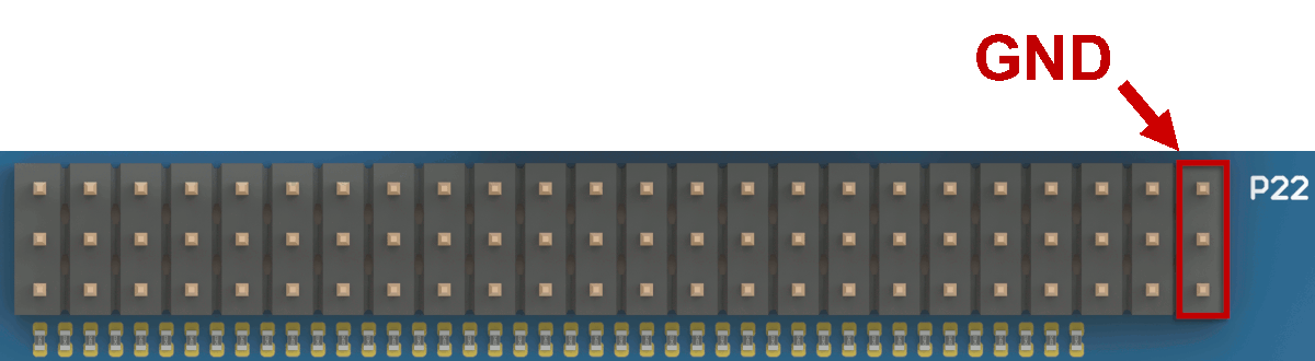
You have to attach GND to the breakout pin headers P21 and P22 12 accordingly, and you have to unplug the jumper from the module power supply pin header P5 5.
Arduino Pin Header🔗
You can power the whole evaluation board using the power pins on Arduino pin header P11 24.
Both the 3.3 V and the 5 V pins can be used.
When you want to use 5 V, you must set the Arduino power direction pin header P17 8 as follows:
Breakout Pin Header🔗
You can power the whole evaluation board using the power pins on breakout pin header P22 25.
Both the 3.3 V and the 5 V pins can be used.
Module Power Options🔗
You can power the module by two different supply voltage modes.
- Normal Voltage Mode using 3.3 V
- High Voltage Mode using 5 V
The mode setting depends on which voltage levels are connected to VCC and VDDH pins on the power configuration pin header P7 11.
Normal Voltage Mode🔗
You can configure the supply voltage mode to Normal Voltage Mode using the power configuration pin header P7 11 as follows:
- Connect 3.3 V to VCC pin
- Connect 3.3 V to VDDH pin
High Voltage Mode🔗
Note
When you use the High Voltage Mode, a current measurement using the current measurement pin header P4 4 is not possible anymore.
You have to use a separate power supply and connect it directly to the VDDH pin of the power configuration pin header P7 11 instead.
You can configure the supply voltage mode to High Voltage Mode using the power configuration pin header P7 11 as follows:
- Connect 5 V to VDDH pin
- Leave VCC pin unconnected
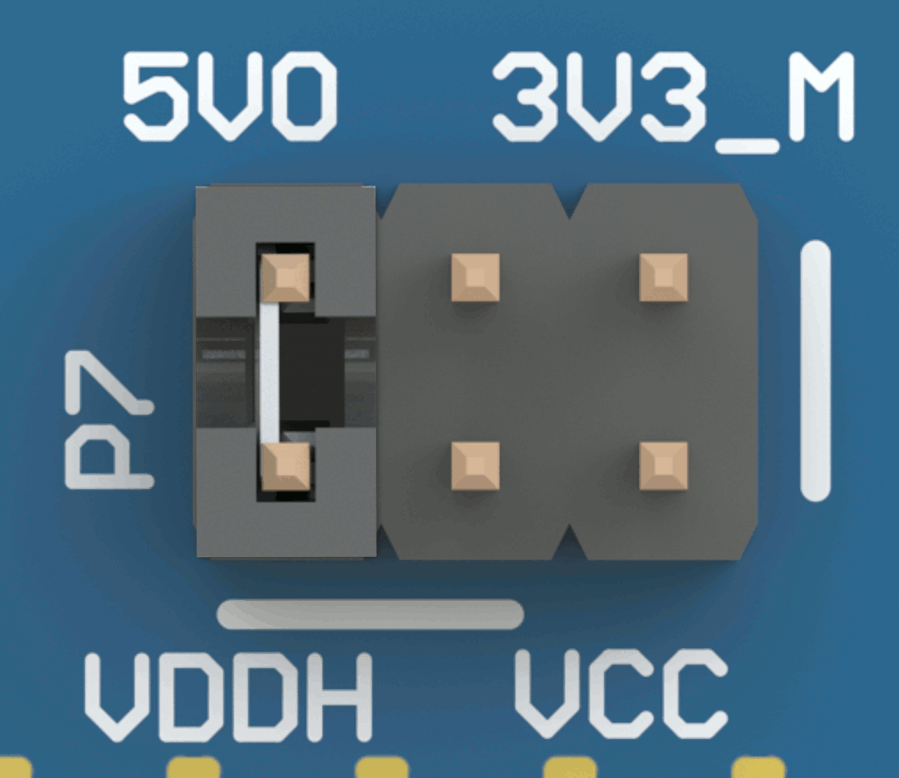
For further information please refer to section 5.3.1 Main Supply in chapter 5.3 POWER - Power Supply in the nRF52840 Product Specification.
GPIO Pin Access🔗
You can access every GPIO pin of the module through the breakout pin headers P21 and P22 12.

For each GPIO pin dedicated pull-up and pull-down pins are available as well which you can bridge using a jumper. This makes it easy to permanently pull GPIO pins to GND or VCC or attach additional circuitry easily.
You can check the details of the pin mappings between the evaluation board, the module and the nRF52840 in the following table.
| EVB Pin | Module Footprint | Module Pin | nRF52840 Footprint | nRF52840 Pin |
|---|---|---|---|---|
| 3.3 V 1 | ||||
| 5 V 2 | ||||
| 0.02 | A6 | P0.02 | B6 | P0.02 |
| 0.03 | A5 | P0.03 | A5 | P0.03 |
| 0.04 | A3 | P0.04 | C10 | P0.04 |
| 0.05 | A4 | P0.05 | D10 | P0.05 |
| 0.06 | B1 | P0.06 | E9 | P0.06 |
| 0.07 | D3 | P0.07 | F9 | P0.07 |
| 0.08 | C1 | P0.08 | E10 | P0.08 |
| 0.09 | A9 | P0.09 | F1 | P0.09 |
| 0.10 | A8 | P0.10 | E2 | P0.10 |
| 0.11 | F2 | P0.11 | H8 | P0.11 |
| 0.12 | F1 | P0.12 | G10 | P0.12 |
| 0.13 | F3 | P0.13 | H7 | P0.13 |
| 0.14 | F4 | P0.14 | J7 | P0.14 |
| 0.15 | F5 | P0.15 | K7 | P0.15 |
| 0.16 | G1 | P0.16 | H6 | P0.16 |
| 0.17 | E4 | P0.17 | J6 | P0.17 |
| 0.19 | F6 | P0.19 | K4 | P0.19 |
| 0.20 | E6 | P0.20 | J5 | P0.20 |
| 0.21 | E7 | P0.21 | J4 | P0.21 |
| 0.22 | F9 | P0.22 | K3 | P0.22 |
| 0.23 | E5 | P0.23 | H5 | P0.23 |
| 0.24 | D6 | P0.24 | H4 | P0.24 |
| 0.25 | F8 | P0.25 | K2 | P0.25 |
| 0.26 | A2 | P0.26 | C9 | P0.26 |
| 0.27 | A1 | P0.27 | D9 | P0.27 |
| 0.28 | B5 | P0.28 | A6 | P0.28 |
| 0.29 | A7 | P0.29 | C7 | P0.29 |
| 0.30 | B3 | P0.30 | A7 | P0.30 |
| 0.31 | B4 | P0.31 | C8 | P0.31 |
| 1.00 | G8 | P1.00 | J3 | P1.00 |
| 1.01 | F7 | P1.01 | J1 | P1.01 |
| 1.02 | D7 | P1.02 | G3 | P1.02 |
| 1.03 | C3 | P1.03 | F3 | P1.03 |
| 1.04 | E9 | P1.04 | H1 | P1.04 |
| 1.05 | C9 | P1.05 | G2 | P1.05 |
| 1.06 | B8 | P1.06 | E3 | P1.06 |
| 1.07 | D8 | P1.07 | G1 | P1.07 |
| 1.08 | D2 | P1.08 | G9 | P1.08 |
| 1.09 | E2 | P1.09 | F10 | P1.09 |
| 1.10 | B7 | P1.10 | B4 | P1.10 |
| 1.11 | C7 | P1.11 | A3 | P1.11 |
| 1.12 | C8 | P1.12 | C5 | P1.12 |
| 1.13 | B6 | P1.13 | A4 | P1.13 |
| 1.14 | C6 | P1.14 | B5 | P1.14 |
| 1.15 | B9 | P1.15 | C6 | P1.15 |
| GND | ||||
1 The maximum output current using 3.3 V is 500 mA.
2 The maximum output current depends on the USB supply.
Arduino Interface🔗
You can use the Arduino interface on the Arduino Arduino pin headers P9, P10, P11, P13 10 to stack the evaluation board with other boards and shields that have an Arduino connector.
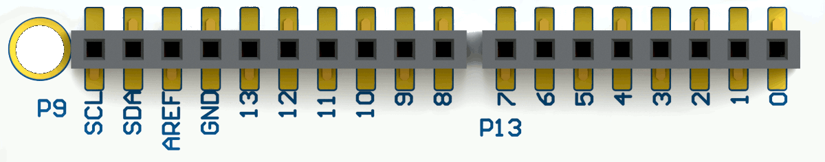
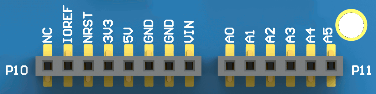
You can check the details of the pin mappings between the evaluation board, the module and the nRF52840 in the following table.
| Arduino Pin | Function | Module Footprint | Module Pin | nRF52840 Footprint | nRF52840 Pin |
|---|---|---|---|---|---|
| IOREF | 3.3 V Ref Voltage Out | ||||
| NRST | Module Reset | G7 | Reset | K6 | P0.18 |
| 3V3 | 3.3 V input/output | The maximum output current is 500 mA. | |||
| 5V | 5 V input/output | The maximum output current depends on the USB supply. | |||
| GND | Ground | ||||
| GND | Ground | ||||
| VIN | Not Connected | ||||
| A0 | Analog Input | A5 | P0.03 | A5 | P0.03 |
| A1 | Analog Input | A3 | P0.04 | C10 | P0.04 |
| A2 | Analog Input | B5 | P0.28 | A6 | P0.28 |
| A3 | Analog Input | A7 | P0.29 | C7 | P0.29 |
| A4 | Analog Input | B3 | P0.30 | A7 | P0.30 |
| A5 | Analog Input | B4 | P0.31 | C8 | P0.31 |
| SCL | I2C Clock | A1 | P0.27 | D9 | P0.27 |
| SDA | I2C Data | A2 | P0.26 | C9 | P0.26 |
| AREF | A6 | P0.02 | B6 | P0.02 | |
| GND | Ground | ||||
| D13 | GPIO | F5 | P0.15 | K7 | P0.15 |
| D12 | GPIO | F4 | P0.14 | J7 | P0.14 |
| D11 | GPIO | F3 | P0.13 | H7 | P0.13 |
| D10 | GPIO | F1 | P0.12 | G10 | P0.12 |
| D9 | GPIO | C7 | P1.11 | A3 | P1.11 |
| D8 | GPIO | B7 | P1.10 | B4 | P1.10 |
| D7 | GPIO | D2 | P1.08 | G9 | P1.08 |
| D6 | GPIO | D8 | P1.07 | G1 | P1.07 |
| D5 | GPIO | B8 | P1.06 | E3 | P1.06 |
| D4 | GPIO | C9 | P1.05 | G2 | P1.05 |
| D3 | GPIO | E9 | P1.04 | H1 | P1.04 |
| D2 | GPIO | C3 | P1.03 | F3 | P1.03 |
| D1 | GPIO / UART RX/TX (depending on P16 setup) | F7/D7 | P1.01/1.02 | J1/G3 | P1.01/1.02 |
| D0 | GPIO / UART TX/RX (depending on P16 setup) | D7/F7 | P1.02/P1.01 | G3/J1 | P1.02/P1.01 |
Arduino Configuration🔗
You can use the evaluation board either as an Arduino board or as an Arduino shield. The main difference between the two is that the UART communication and the 5 V power configuration are changed.
Note
In the default configuration the evaluation board is configured as Arduino board.
You can configure the UART communication by using the Arduino UART direction pin header P16 18 which will flip the Rx and Tx direction of the UART communication.
You can configure the 5 V power configuration by using the Arduino power direction pin header P17 8 which configures a diode to block the input power accordingly.
Board Configuration🔗
You can configure the evaluation board to Arduino board configuration as follows:
-
Set the Arduino UART direction pin header P16 18 as shown
-
Set the Arduino power direction pin header P17 8 as shown

Shield Configuration🔗
You can configure the evaluation board to Arduino shield configuration as follows:
-
Set the Arduino UART direction pin header P16 18 as shown
-
Set the Arduino power direction pin header P17 8 as shown
Peripheral Configuration🔗
You can enable or disable some of the peripheral components on the evaluation board by using the peripheral disable pin header P6 23, for example, to aid current consumption measurements.
The following peripherals will always be enabled, regardless of the setting of the peripheral disable pin header P6 23:
- The module itself
- Reset button
- User buttons
- User LEDs
- Power from USB connector X1 1
- Current measurement interface
- Module native USB interface
- Arduino interface
- Breakout pin interface
Enable Peripherals🔗
You can enable the power to all of the peripheral components as follows:
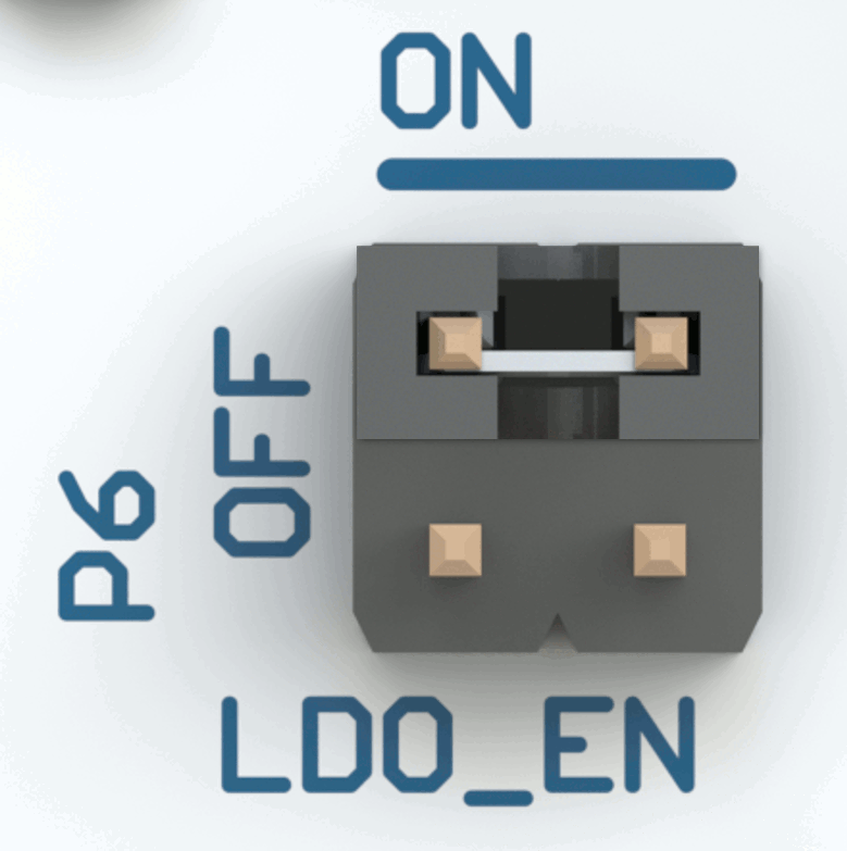
Disable Peripherals🔗
You can disable power to some of the peripheral components as follows to save energy when it is powered from a battery or power-bank for example:
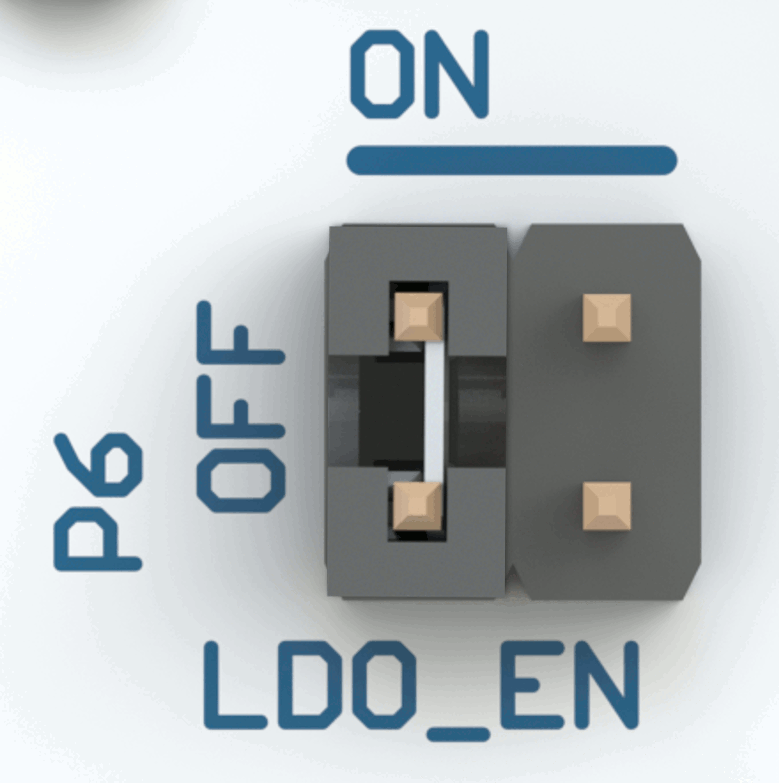
The following peripheral components will be disabled:
- Segger J-Link on-board debugger
Current Consumption Measurement🔗
You can measure the current consumption of the module independently of the peripheral components.
Note
Before any current consumption measurement, you have to cut the power supply to the module using the module power supply pin header P5 5, otherwise, the current consumption measurement will not work.
Tip
If you do not have any equipment for current consumption measurement, check out the Power Profiler Kit II from Nordic Semiconductor, which can be used both as an ammeter and source meter.
Using an Ammeter🔗
For a current consumption measurement using an ammeter you have to execute the following steps:
-
Remove the jumper from the module power supply pin header P5 5 to disconnect the power supply from the module:
-
Connect the ammeter to current measurement pin header P4 4 as follows:
-
Put a jumper to the peripheral disable pin header P6 23 to deactivate the peripheral components.

Now you have two choices to power the board.
-
Power the board regularly using the USB connector X1 1.
-
Power the board using a variable voltage power supply by feeding directly into GND and 3.3 V on the breakout pin headers P21 and P22 12 to be able to simulate different battery voltage levels.
Using a Source Meter🔗
For a current consumption measurement using a source meter you have to execute the following steps:
-
Remove the jumper from the module power supply pin header P5 5 to disconnect the power supply from the module.
-
Connect the source meter to current measurement pin header P4 4 as follows:
-
Put a jumper to the peripheral disable pin header P6 23 to deactivate the peripheral components.

-
Power the board using the USB connector X1 1.
Warning
You have to power the board additionally using the USB connector X1 1.
The jumper put on the peripheral disable pin header P6 23 disconnects certain peripheral components from the module by switching multiple analog switches. But for this to work, the analog switches themselves must be powered using the USB connector X1 1.
Otherwise, signal lines that are connected to the analog switches may float which may result in unexpected behavior and incorrect current consumption measurements in the end.
Software Development🔗
Warning
This module is radio certified. There are conditions on hardware and software which must be met for a valid usage of the certification.
For further information please refer to the module-specific product specification at
Nordic Semiconductor provides several software development kits (SDK) with building tools and sample projects.
For further information please refer to the Software Documentation from Nordic Semiconductor.
nRF Connect SDK🔗
The nRF Connect SDK contains the pan1780_evb board definition which you can use when adding a build configuration to a project.
Bluetooth Device Address Safeguard🔗
Each module is pre-programmed and comes with a public Bluetooth Device Address and a random Bluetooth Device Address. Both can be easily used in applications, depending on the anticipated use case.
All applications from the nRF Connect SDK automatically use the built in random Bluetooth Device Address, but can easily be modified when the public Bluetooth Device Address shall be used.
Before starting development, it is necessary to read out the module specific information, so that it can be restored whenever needed.
During development, it is sometimes necessary to reset the module to the factory default state (“erase all”). This will also reset all the pre-programmed information in the module.
So special care must be taken that the public Bluetooth Device Address is not accidentally erased and lost, even if the public Bluetooth Device Address is not explicitly used during evaluation of the evaluation board.
Background Information🔗
During production of the module, some module specific information is stored in the user information configuration registers (UICRs) of the module.
UICRs are non-volatile memory (NVM) registers for configuring user specific settings and can be modified by the user.
The module specific information in the UICRs include:
- Public Bluetooth Device Address
- Hardware Revision
Panasonic Bluetooth Device Address Ranges
The Bluetooth Device Address of the module always starts with one of these prefixes:
-
00:13:43 - Matsushita Electronic Components (Europe) GmbH
-
34:32:e6 - Panasonic Industrial Devices Europe GmbH
This module specific information is also encoded in the 2D barcode on the metal shield box on the module. The 2D barcode can only be read with a suitable barcode reader.
All module specific information is stored in the registers CUSTOMER[0] and CUSTOMER[1] of the UICR during production.
The UICRs behave like a single block of flash memory, i.e. they can only be written at once, and they can only be erased as a whole.
Whenever the module is reset to the factory default state (“erase all”), this will also reset the UICRs. Thus all module specific information is deleted that was stored during the production of the module.
Saving Production Information🔗
Warning
Please note that every module has a unique Bluetooth Device Address, so this step must be done for every module individually.
To save all module specific information that is programmed during the production of the module, it is sufficient to read out the UICR registers CUSTOMER[0] and CUSTOMER[1].
The following requirement must be met:
- nRF Util Development Tool is installed.
-
Use the
nrfutiltool from a command line prompt to read the first half of the module specific information.nrfutil.exe device read --address 0x10001080The output should look something like this:
0x10001080: E6AABBCC |....| -
Use the
nrfutiltool again to read the second half of the module specific information.nrfutil.exe device read --address 0x10001084The output should look something like this:
0x10001084: 01023432 |....|
These two values are unique and must be stored safely.
Restoring Production Information🔗
Warning
To modify already written portions of the UICR, the complete UICR area must be erased before.
To restore the previously saved module specific information, it is sufficient to write back the stored information into the UICR registers CUSTOMER[0] and CUSTOMER[1].
The following requirement must be met:
- nRF Util Development Tool is installed.
-
Use the
nrfutiltool from a command line prompt and restore the first half of the module specific information that was previously saved.nrfutil.exe device write --address 0x10001080 --value 0xE6AABBCCThe output should look something like this:
v Data written to <serial-number> -
Use the
nrfutiltool again and restore the second half of the module information that was previously saved.nrfutil.exe device write --address 0x10001084 --value 0x01023432The output should look something like this:
v Data written to <serial-number>