User Guide🔗

Introduction🔗
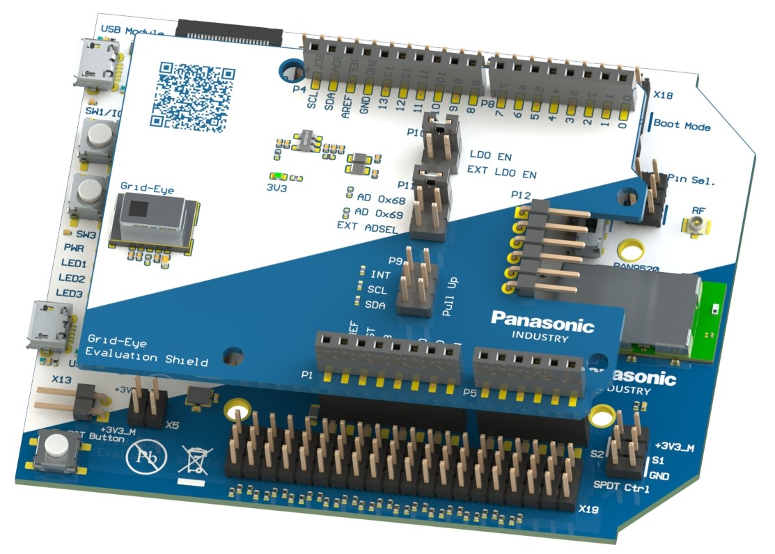
The PAN9520 evaluation board (ENW49D01AZKF) features a PAN9520 which is a 2.4 GHz 802.11 b/g/n embedded Wi‑Fi module based on the Espressif ESP32-S2 single-chip controller.
You can access all the different module interfaces like USB, UART, JTAG, GPIOs, and current consumption measurement pins easily, which makes the evaluation board ideally suited for the evaluation of the module and rapid prototyping of products.
Grid-EYE Connectivity Kit
You can use the Arduino interface to easily attach ready-to-run external sensor shields.
For example, Grid-EYE is an infrared thermophile array temperature sensor that is available in narrow, stand and wide angle variants.
For more information you can visit the Grid-EYE product pages at
You can check out the Grid-EYE Connectivity Kit that bundles a PAN9520 evaluation board with one of the Grid-EYE variants on an Arduino shield.
For more information you can visit the Grid-EYE Connectivity Kit product pages at
Features🔗
- Based on module variant ENW49D01A1KF with 4 MB of QSPI Flash and 2 MB of QSPI PSRAM
- Arduino interface configurable as shield or board
- 4x user buttons, 3x user LEDs
- Camera interface
- Module native USB interface
- All GPIOs accessible via pin headers
- Current measurement interface
- FTDI FT2232 USB dual interface
- USB to JTAG
- USB to UART0
- FTDI FT232 USB to UART1 interface
- Peripherals can be deactivated for low power applications
Block Diagram🔗

Board Overview🔗

1
Module native USB connector
You can use the module native USB connector to interact with the USB interface of the module. It is directly connected to the USB pins of the module. Also see Powering Options
2
SW1/IO0 boot button
Use button SW1 for controlling the boot mode at start-up or as general-purpose button in application.
3
User buttons
You can use the user buttons to interact with the running application if the application supports it.
4
User LEDs pin header - X3
You can use this pin header to disconnect the LEDs from the module GPIOs
5
Power LED
The power LED shows you that the board is correctly powered.
6
User LEDs
You can use the user LEDs from the application to interact with the user.
7
USB Debug/Serial connector
With the USB connector you can power the board and gain access to the UART communication and debugging capabilities.
8
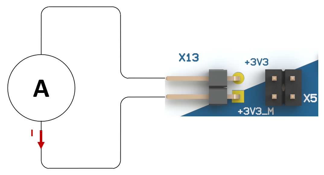
Current measurement pin header - X13
The current measurement pin header offers you the possibility to measure the current consumption of the currently running application.
9
Reset button
You can use the reset button to reset the board to a known-good state.
10
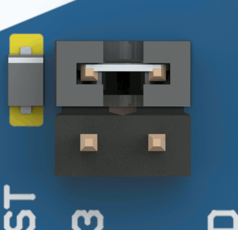
Peripheral power supply
The peripheral disable pin header allows you to control the connection of the USB hub and the two FTDI adapters to the power supply. This is useful for disconnecting these peripherals for current consumption measurements.
11
Module power supply pin header - X5
This pin header allows you to open the current path to the module for current measurement purposes
12
USB hub IC
USB hub which connects the FT232 and the FT2232 to the USB connector. This allows you to only use one USB connector to access three interfaces.
13
FT2232 IC (JTAG and UART0)
USB to dual port converter. Gives you access to JTAG and UART0 interfaces (port0: JTAG, port1: UART0).
14
5V input/output control pin header
You can use the Arduino power direction pin header to configure the operation when using the Arduino pin headers.
15
Power pins on Arduino pin header
You can use these power pins on the Arduino pin header to power the board.
16
Break out pin header - X18 / X19
The breakout pin headers gives you access to all the module GPIO pins directly.
17
Arduino interface
You can use the Arduino pin headers to attach Arduino shields or boards.
18
JTAG signals
Over the JTAG pin header you can access the connection of the JTAG interface, which is directly connected to the JTAG module pins.
19
Power pins on breakout pin header
You can use these power pins on the breakout pin header to power the board.
20
SPDT control pin header
With this pin header you can control the SPDT RF switch on the PAN9520.
21
PAN9520 module
PAN9520 802.11 b/g/n embedded Wi-Fi module
22
USB IO switch
You can use this switch to choose if the module USB pins should be connected to the native USB connector or to the break out pin header.
23
U.FL connector
Here you can attach an antenna if the module's RF Pad is used as RF output interface.
24
Arduino UART signal direction control pin header
You can use the Arduino UART direction pin headers to choose the configuration when running in shield or board mode.
25
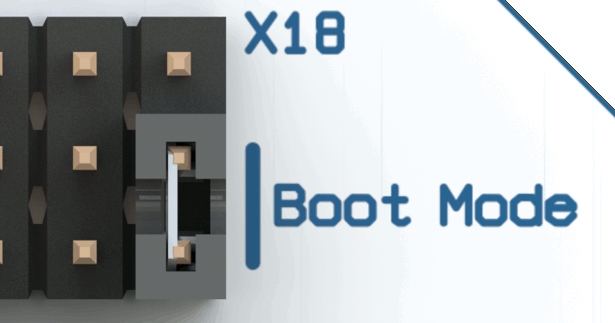
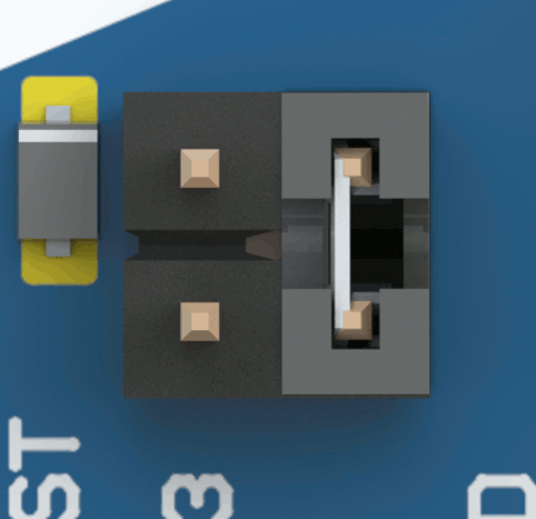
GPIO0/boot pull-up jumper
You must connect the pull-up on GPIO0 for entering the application boot mode per default when powering the module, .
26
UART0/program pin header
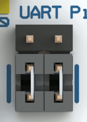
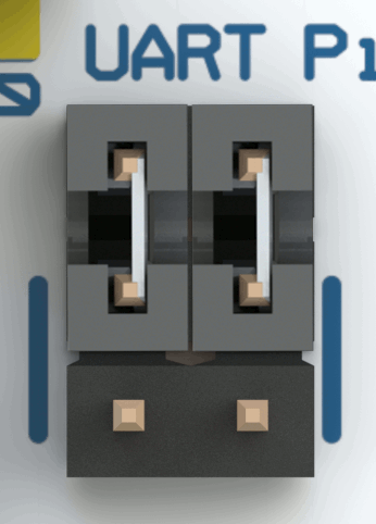
With this pin header you can access and/or separate the connection between the FT2232 and the module pins UART0 (TX and RX), RSTn (DTR controlled), and IO0 (RTS controlled).
27
UART1 pin header
With this pin header you can access and/or separate the connection between the FT232 and the module's UART1 signals (TX, RX, CTS, RTS).
28
I²C pull-up pin header
You can connect 4.7 kΩ pull-up resistors to GPIO7 and GPIO8 with this pin header. GPIO7 and GPIO8 are used for I²C on the Arduino socket and camera connector.
29
Camera voltage control 1.2 to 1.8 V
Low supply voltage control of camera interface. You can configure 1.2 V, 1.5 V, and 1.8 V by several jumper settings.
30
Camera voltage control 2.8 to 3.3 V
High supply voltage control of camera interface. You can configure 2.8 V, 3 V, and 3.3 V by several jumper settings.
31
Camera interface
Here you can connect different camera modules.
32
FT232 IC (UART1)
USB to serial converter which gives you access to UART1 interface.
Initial Preparations🔗
Before you can work with the evaluation tool (again) you may have to check (or restore) the default jumper configuration or install device drivers, depending on the operating system you are using.
Default Jumper Configuration🔗
You can check the default jumper configuration easily because it is imprinted with white (or blue) line markings on the silkscreen of the PCB.
For example, the default jumper configuration in the following picture is:
- One jumper put on the lower left two pins
- One jumper put on the lower right two pins
FTDI USB UART Driver🔗
You may have to install a driver for the FTDI USB UART if the operating system you are using does not provide one automatically.
If in doubt, please refer to the FTDI website and install the drivers manually. For further information please refer to FTDI Driver Page.
Powering Options🔗
You can power the evaluation board in different ways:
- USB Debug/Serial connector 7
- Module native USB connector 1
- current measurement pin header X13 8
- power pins on Arduino pin header 15
- power pins on breakout pin header 19
Risk of damaging board components
Do not supply 5 V on the 3.3 V pin of the power pins on Arduino pin header 15 or the power pins on breakout pin header 19.
USB Connector🔗
You can power the whole evaluation board using the USB Debug/Serial connector 7.
Note
Please note that the module is still powered if the peripherals are deactivated using peripheral power supply 10.
Module Native USB Connector🔗
You can power the whole evaluation board using the Module native USB connector 1.
Note
Please note that the module is still powered if the peripherals are deactivated using peripheral power supply 10.
Current Measurement Pin Header🔗
You can power the module by attaching VCC to the current measurement pin header X13 8.
You have to attach GND to the break out pin header X18 / X19 16 accordingly, and you have to unplug the jumper from the module power supply pin header X5 11.

Arduino Pin Header🔗
You can power the whole evaluation board using the power pins on Arduino pin header 15.
Both the 3.3 V and the 5 V pins can be used.
When you want to use 5 V, you must set the 5V input/output control pin header 14 as follows:

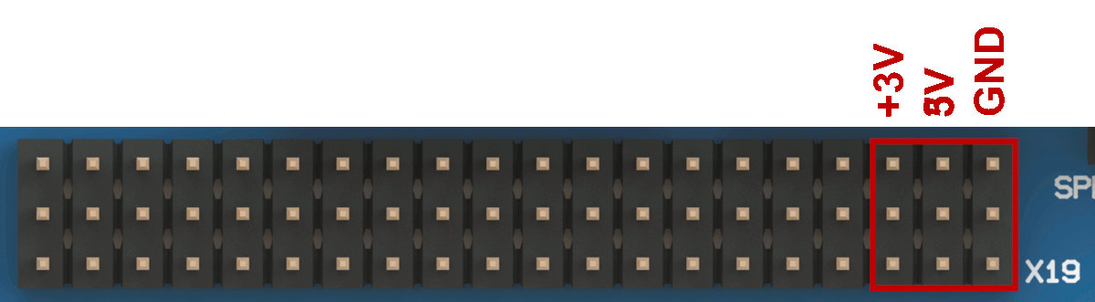
Breakout Pin Header🔗
You can power the whole evaluation board using the power pins on breakout pin header 19.
Both the 3.3 V and the 5 V pins can be used.
Default Boot Mode🔗
Pull-Up GPIO0
It is recommended that you connect a pull-up resistor on GPIO0 by using the GPIO0/boot pull-up jumper 25. This ensures that the PAN9520 boots the loaded application directly after powering the device.
Workaround
Please note that the described setting shall ensure that the default application boot mode is also entered directly after powering the board. This default mode is also set by the ESP32-S2, but does only work, if the device is already powered and then reset.
Use SW1 for entering the download mode SW1/IO0 at Start-Up.
At the start-up of the PAN9520, the ESP32-S2 evaluates the so-called strapping pins. The default values of the strapping pins are determined by internal pull-resistors of the ESP32-S2. These work fine for start-ups caused by resets.
If you power the PAN9520, the pull-resistors need some time to be configured and the device does not start in the default mode. This is especially important to note for GPIO0, which configures the boot mode after start-up.
It is recommended to connect the related pull-up resistor on GPIO0, for ensuring that the PAN9520 boots the loaded application after you have powered the board. The caption "Boot Mode" on the PAN9520 EVB indicates the corresponding jumper placement.
If you don't place the jumper, the module enters the download mode after powering and an additional reset is needed to start the device in the usual application boot mode.
For further information on the strapping pins and boot options please refer to the PAN9520 Product Specification at
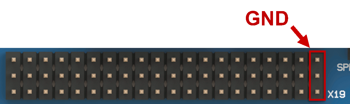
Breakout Pin Header🔗
You can access every GPIO pin of the module through the break out pin header X18 / X19 16.
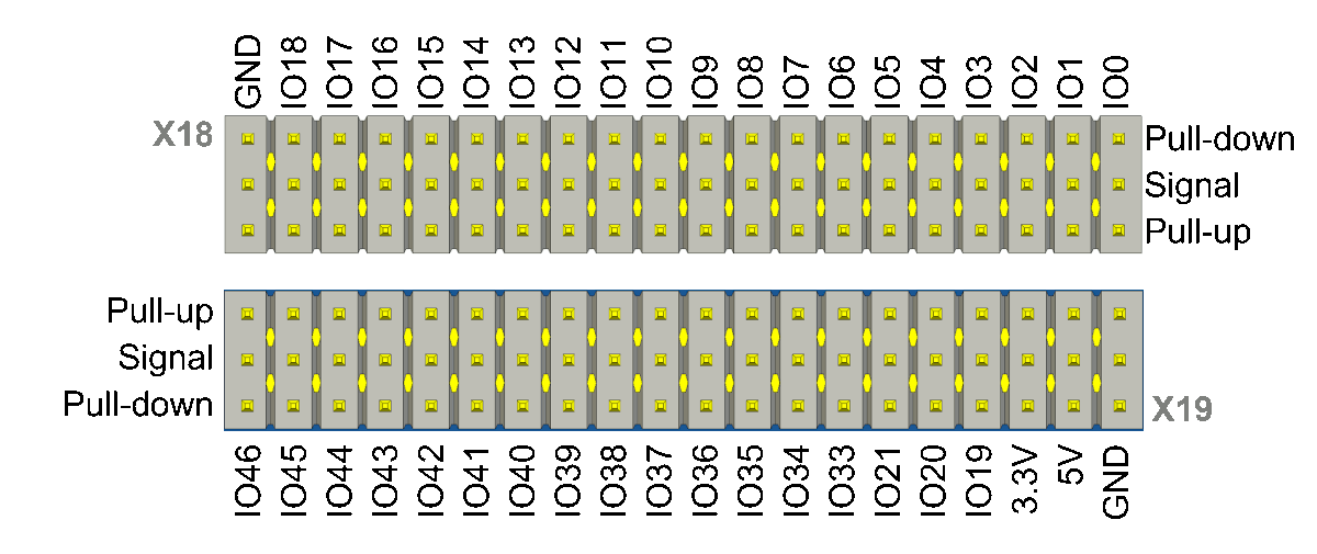
Dedicated pull-up and pull-down pins are available for each GPIO pin. You can bridge them by using a jumper. This makes it easy to permanently pull GPIO pins to GND or VCC or attach additional circuitry easily.
You can check the details of the pin mappings between the breakout pin header, the module and the ESP32-S2 in the following table.
| EVB Pin | PAN9520/ESP32-S2 Pin Name | PAN9520 Footprint | ESP32-S2 Footprint |
|---|---|---|---|
| IO0 | GPIO0 | I11 | 5 |
| IO1 | GPIO1 | B11 | 6 |
| IO2 | GPIO2 | C11 | 7 |
| IO3 | GPIO3 | C12 | 8 |
| IO4 | GPIO4 | C13 | 9 |
| IO5 | GPIO5 | D11 | 10 |
| IO6 | GPIO6 | D13 | 11 |
| IO7 | GPIO7 | E11 | 12 |
| IO8 | GPIO8 | E12 | 13 |
| IO9 | GPIO9 | E13 | 14 |
| IO10 | GPIO10 | F13 | 15 |
| IO11 | GPIO11 | F11 | 16 |
| IO12 | GPIO12 | G13 | 17 |
| IO13 | GPIO13 | G12 | 18 |
| IO14 | GPIO14 | B11 | 19 |
| IO15 | XTAL_32K_P | I10 | 21 |
| IO16 | XTAL_32K_N | I9 | 22 |
| IO17 | DAC_1 | I8 | 23 |
| IO18 | DAC_2 | I7 | 24 |
| IO19 | GPIO19 | H7 | 25 |
| IO20 | GPIO20 | H6 | 26 |
| IO21 | GPIO21 | H11 | 28 |
| IO33 | GPIO33 | C1 | 37 |
| IO34 | GPIO34 | B1 | 38 |
| IO35 | GPIO35 | A2 | 39 |
| IO36 | GPIO36 | A3 | 40 |
| IO37 | GPIO37 | A4 | 41 |
| IO38 | GPIO38 | A5 | 42 |
| IO39 | MTCK | E1 | 43 |
| IO40 | MTDO | F1 | 44 |
| IO41 | MTDI | G1 | 46 |
| IO42 | MTMS | H1 | 47 |
| IO43 | U0TXD | A7 | 48 |
| IO44 | U0RXD | A8 | 49 |
| IO45 | GPIO45 | A10 | 50 |
| IO46 | GPIO46 | A11 | 55 |
| 3.3 V 1 | |||
| 5 V 2 | |||
| GND | |||
1 The maximum output current is 500 mA.
2 The maximum output current depends on the USB supply.
User LEDs🔗
There are three LEDs you can use for general purposes on the PAN9520 EVB.
The LEDs are connected to GPIOs via user LEDs pin header X3 4. You can disconnect every LED by unplugging the related jumper.
The following figure and table show details on the assigned pins.
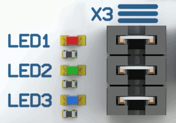
| LED | Color | PAN9520/ESP32-S2 Pin Name | PAN9520 Footprint | ESP32-S2 Footprint |
|---|---|---|---|---|
| LED1 | Red | GPIO21 | H11 | 28 |
| LED2 | Green | GPIO33 | C1 | 37 |
| LED3 | Blue | GPIO38 | A5 | 42 |
User Buttons🔗
You can use four user buttons 3 for interaction with the PAN9520. For additional functionality of the SW1/IO0 boot button 2 please refer to SW1/IO0 at Start-Up.
If you press a button, the corresponding GPIO connects to ground level, which makes the buttons active-low. If you need pull-up resistors, you can either configure this by software, or connect them externally by using jumpers on the GPIO breakout header. For details please refer to Breakout Pin Header.
The following table describes which GPIOs are connected to the buttons.
| Button Name | PAN9520/ESP32-S2 Pin Name | PAN9520 Footprint | ESP32-S2 Footprint |
|---|---|---|---|
| SW1/IO0 | GPIO0 | I11 | 5 |
| SW2 | GPIO1 | B11 | 6 |
| SW3 | GPIO2 | C11 | 7 |
| SW4 | GPIO3 | C12 | 8 |
SW1/IO0 at Start-Up🔗
Pull-Up GPIO0
It is recommended that you connect a pull-up resistor on GPIO0 by placing the GPIO0/boot pull-up jumper 25. This ensures that the PAN9520 boots the loaded application directly after powering the device.
If you powered the device already and reset, the default application boot mode is also configured by an ESP32-S2 internal pull-up resistor.
At start-up, the voltage level on GPIO0 is evaluated for configuring the boot mode. If the voltage level is high, the device enters the usual application boot mode. If the voltage level is low, the device enters the download mode, which allows loading software to the PAN9520 .
Because SW1 is connected to GPIO0, you can use the button for entering this download mode manually. Therefore, you must press SW1 while resetting the module.
IO0 is Controlled by FT2232
Usually, it is not required to set the boot mode manually when you use UART0 as interface for downloading the firmware into the PAN9520. In this case, IO0 and RSTn are controlled by the USB-to-UART0 interface of the FT2232.
For further information please refer to Default Boot Mode and the PAN9520 Product Specification at
Arduino Interface🔗
You can use the Arduino interface 17 to stack the EVB with other boards and shields with Arduino connectors.
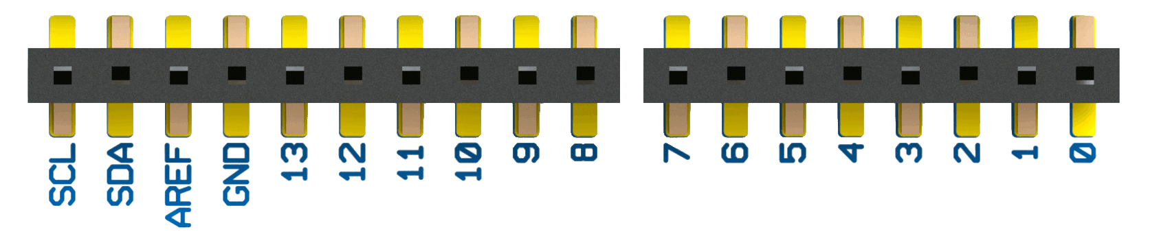
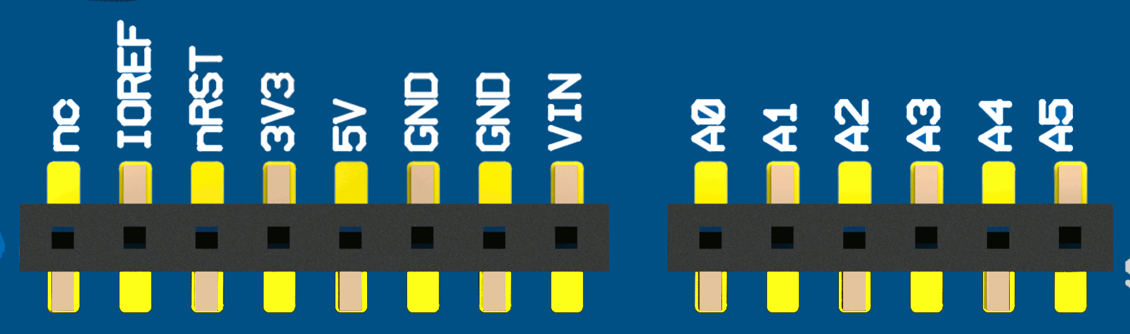
You can check the details of the pin mappings between the evaluation board, the module and the ESP32-S2 in the following table.
| Arduino Pin | Function | PAN9520/ESP32-S2 Pin Name | PAN9520 Footprint | ESP32-S2 Footprint |
|---|---|---|---|---|
| IOREF | 3.3 V Ref Voltage Out | |||
| NRST | Module Reset | CHIP PU | A12 | 56 |
| 3V3 1 | ||||
| 5V 2 | ||||
| GND | Ground | |||
| GND | Ground | |||
| VIN | Not Connected | |||
| A0 | Analog Input | GPIO1 | B11 | 6 |
| A1 | Analog Input | GPIO2 | C11 | 7 |
| A2 | Analog Input | GPIO3 | C12 | 8 |
| A3 | Analog Input | GPIO4 | C13 | 9 |
| A4 | Analog Input | GPIO5 | D11 | 10 |
| A5 | Analog Input | GPIO6 | D13 | 11 |
| SCL | I2C Clock | GPIO7 | E11 | 12 |
| SDA | I2C Data | GPIO8 | E12 | 13 |
| AREF | Not connected | |||
| GND | Ground | |||
| D13 | GPIO/SPI_SCK | GPIO36 | A3 | 40 |
| D12 | GPIO/SPI_MISO | GPIO37 | A4 | 41 |
| D11 | GPIO/SPI_MOSI | GPIO35 | A2 | 39 |
| D10 | GPIO/SPI_SS | GPIO34 | B1 | 38 |
| D9 | GPIO | GPIO9 | E13 | 14 |
| D8 | GPIO | GPIO10 | F13 | 15 |
| D7 | GPIO | GPIO11 | F11 | 16 |
| D6 | GPIO | GPIO12 | G13 | 17 |
| D5 | GPIO | GPIO13 | G12 | 18 |
| D4 | GPIO | GPIO14 | G11 | 19 |
| D3 | GPIO | GPIO15 (XTAL_32K_P) | I10 | 21 |
| D2 | GPIO | GPIO16 (XTAL_32K_N) | I9 | 22 |
| D1 | GPIO / UART RX 3 | GPIO17 (DAC_1) | I8 | 23 |
| D0 | GPIO / UART TX 3 | GPIO18 (DAC_2) | I7 | 24 |
1 3.3 V input/output - The maximum output current is 500 mA.
2 5 V input/output - The maximum output current depends on the USB supply.
3 Depending on setup of Arduino UART signal direction control pin header 24 described in section Arduino Configuration.
Arduino Configuration🔗
You can use the evaluation board either as an Arduino board or as an Arduino shield. The main difference between the two is that the UART communication and the 5 V power configuration are changed.
Note
In the default configuration the evaluation board is configured as Arduino board.
You can configure the UART communication by using the Arduino UART signal direction control pin header 24 which will flip the Rx and Tx direction of the UART communication.
You can configure the 5 V power configuration by using the 5V input/output control pin header 14 which configures a diode to block the input power accordingly.
Board Configuration🔗
You can configure the evaluation board to Arduino board configuration as follows:
-
Set the Arduino UART signal direction control pin header 24 as shown
-
Set the 5V input/output control pin header 14 as shown
Shield Configuration🔗
You can configure the evaluation board to Arduino shield configuration as follows:
-
Set the Arduino UART signal direction control pin header 24 as shown
-
Set the 5V input/output control pin header 14 as shown
Peripheral Configuration🔗
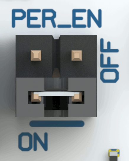
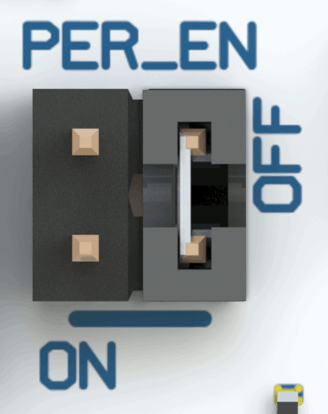
You can enable or disable some of the peripheral components on the evaluation board by using the peripheral power supply 10. For example, to aid current consumption measurements by avoiding current flow through the signal lines of the peripherals.
The following table shows the status of the evaluation board components when the peripheral power supply 10 is in "Disabled" configuration.
| Component | Status |
|---|---|
| USB hub | Disabled |
| FT232 USB to UART interface (UART1) | Disabled |
| FT2232 USB to dual interface (JTAG and UART0) | Disabled |
| User buttons | Enabled |
| Reset button | Enabled |
| Powering via peripheral USB | Enabled |
| User LEDs | Enabled |
| Current consumption measurement | Enabled |
| PAN9520 | Enabled |
| Module native USB interface | Enabled |
| Arduino interface | Enabled |
| Breakout pins | Enabled |
| Camera interface | Enabled |
Enable Peripherals🔗
If you want to enable the power to all of the peripheral components place the jumper as shown:
Disable Peripherals🔗
For disabling the power to some of the peripheral components place the jumper as shown:

This saves energy when it is powered from a battery or power-bank for example, or if you want to measure the current consumption.
Current Consumption Measurement🔗
You can measure the current consumption of the module independently of the peripheral components.
Note
Before any current consumption measurement, you have to cut the power supply to the module using the module power supply pin header X5 11, otherwise, the current consumption measurement will not work.
Tip
If you do not have any equipment for current consumption measurement, check out the Power Profiler Kit II from Nordic Semiconductor, which can be used both as an ammeter and source meter.
Using an Ammeter🔗
For a current consumption measurement using an ammeter you have to execute the following steps:
-
Remove the jumper from the module power supply pin header X5 11 to disconnect the power supply from the module:
-
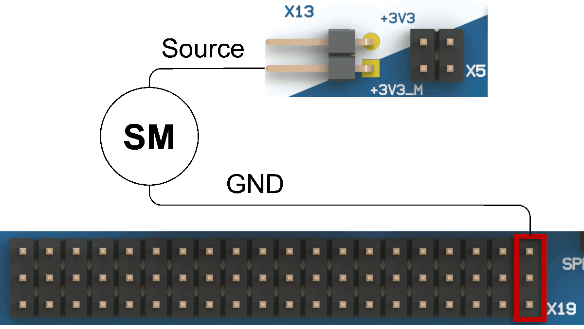
Connect the ammeter to current measurement pin header X13 8 as follows:
-
Put a jumper to the peripheral power supply 10 to deactivate the peripheral components.
Now you have two choices to power the board.
-
Power the board regularly using the USB Debug/Serial connector 7.
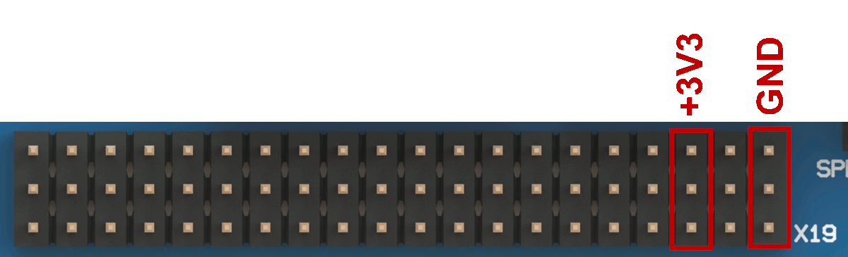
-
Power the board using a variable voltage power supply by feeding directly into GND and 3.3 V on the break out pin header X18 / X19 16 to be able to simulate different battery voltage levels.
Using a Source Meter🔗
For a current consumption measurement using a source meter you have to execute the following steps:
-
Remove the jumper from the module power supply pin header X5 11 to disconnect the power supply from the module.
-
Connect the source meter to current measurement pin header X13 8 as follows:
-
Put a jumper to the peripheral power supply 10 to deactivate the peripheral components.

-
Power the board using the USB Debug/Serial connector 7.
Warning
You have to power the board additionally using the USB Debug/Serial connector 7.
The jumper put on the peripheral power supply 10 disconnects certain peripheral components from the module by switching multiple analog switches. But for this to work, the analog switches themselves must be powered using the USB Debug/Serial connector 7.
Otherwise, signal lines that are connected to the analog switches may float which may result in unexpected behavior and incorrect current consumption measurements in the end.
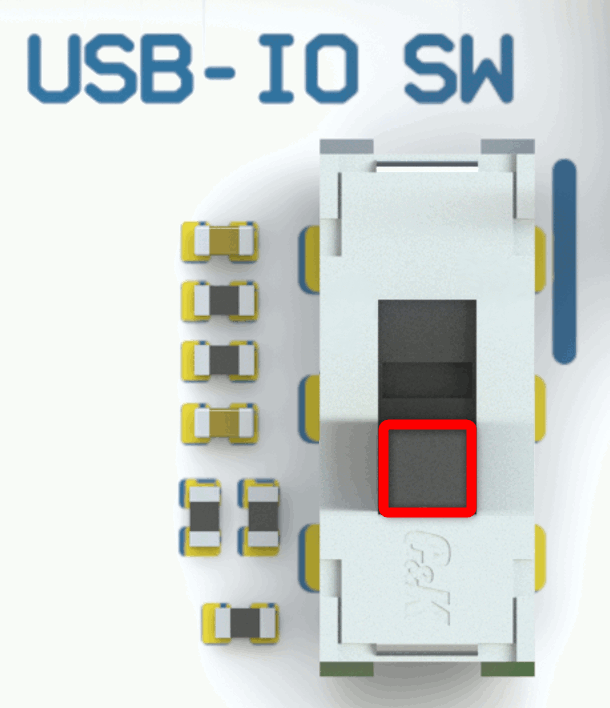
USB-IO Switch🔗
You can configure GPIO19 and GPIO20 to work as native USB interface. They are connected to the Module native USB connector 1 connector.
To avoid bad signal integrity, caused by stubs or other disturbances, you can disconnect all other peripherals from these USB signal lines. Therefore, the USB IO switch 22 is used. It connects a set of USB-related pull-resistors (when you want to use the USB functionality) or the additional periphery (breakout pin header, FT232 RTS, CTS signals) to the USB lines (when you want to use GPIO19 and GPIO20 for anything else).
USB-IO Switch upper position🔗
Peripherals are connected to the USB traces and thus GPIO19 and GPIO20. Connected peripherals are the breakout pin header and CTS/RTS lines of the FT232 USB to UART1 converter (can be still disconnected by pin header UART1).
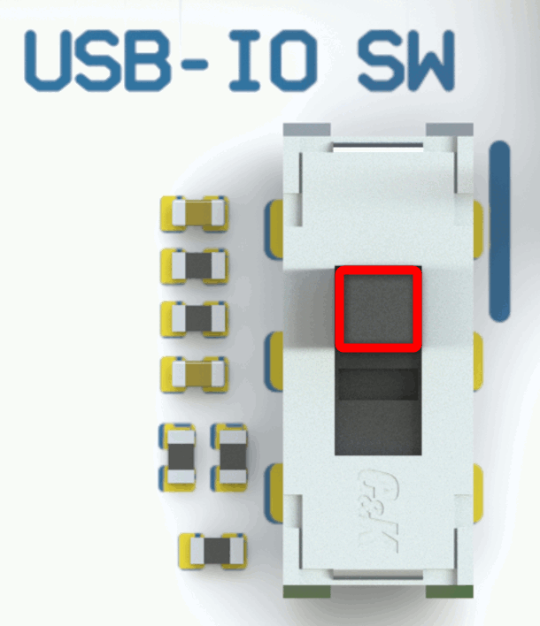
USB-IO Switch lower position🔗
All peripherals are disconnected from the USB traces. Instead, a 1.5 kΩ pull-up resistor is connected to USB D+ (GPIO20), which is the configuration for a full-speed USB device.
I²C Pull-Up Resistors🔗
GPIO7 and GPIO8 are connected to the I²C pins on the Arduino interface 17 and to the SCCB (Serial Camera Control Bus) pins on the camera interface 31. Therefore, 4.7 kΩ pull-up resistors are connected to these GPIOs per default. You can disconnect them by unplugging the I²C pull-up pin header 28 jumpers.
Camera Interface🔗
Disconnect UART1 Jumpers
If you want to use the camera interface 31, disconnect the jumpers on the UART1 pin header 27. For details, please refer to Disconnecting the FT232.
Pin Assignment🔗
The evaluation board contains a 24-pin FPC camera interface 31 for operating a camera module via an 8-bit parallel camera interface and Serial Camera Control Bus (SCCB).
| Camera Pin | Function | PAN9520/ESP32-S2 Pin Name | PAN9520 Footprint | ESP32-S2 Footprint |
|---|---|---|---|---|
| 1 | Not connected | |||
| 2 | Not connected | |||
| 3 | D4 | DAC_2 (GPIO18) | I7 | 24 |
| 4 | D3 | DAC_1 (GPIO17) | I8 | 23 |
| 5 | D5 | XTAL_32K_N (GPIO16) | I9 | 22 |
| 6 | D2 | XTAL_32K_P (GPIO15) | I10 | 21 |
| 7 | D6 | GPIO14 | G11 | 19 |
| 8 | PCLK | GPIO13 | G12 | 18 |
| 9 | D7 | GPIO12 | G13 | 17 |
| 10 | GND (digital) | |||
| 11 | D8 | GPIO11 | F11 | 16 |
| 12 | XCLK | GPIO10 | F13 | 15 |
| 13 | D9 | GPIO6 | D13 | 11 |
| 14 | +3V3 (DOVDD) | |||
| 15 | 1V2-1V8 (DVDD) | |||
| 16 | HREF | GPIO5 | D11 | 10 |
| 17 | PWDN | GPIO4 | C13 | 9 |
| 18 | VSYNC | GPIO3 | C12 | 8 |
| 19 | RST_N (permanent pull-up) | |||
| 20 | SIOC (SCCB clock) | GPIO7 | E11 | 12 |
| 21 | 2V8-3V3 (AVDD) | |||
| 22 | SIOD (SCCB data) | GPIO8 | E12 | 13 |
| 23 | GND (analog) | |||
| 24 | Not connected | |||
Disconnecting the FT232🔗
GPIO17 and GPIO18 are used as data lines for the camera interface. Besides, they are also the default UART1 RX and TX pins which are connected to the FT232 USB to serial transceiver.
Note
If you want to use the camera interface 31, you must disconnect the FT232 from the data lines to ensure that the camera does not transmit data through that interface. Disconnecting the FT232.
If you connect the EVB via the USB Debug/Serial connector 7, this data stream may cause your PC (observed on Windows) to interpret the evaluation board as serial mouse. As a result, unwanted cursor movements and actions take place. If this happens, you should disconnect the EVB again to stop the unwanted behavior.
If you use the camera interface, you must the disconnect the FT232 from the data lines by unplugging the jumpers of the UART1 pin header 27:
Supply Voltage🔗
To support a variety of camera modules with different image sensors, you can configure different voltage levels for the digital core voltage (DVDD), and analog voltage (AVDD) via the pin headers camera voltage control 1.2 to 1.8 V 29 and camera voltage control 2.8 to 3.3 V 30. The following chapters describe the voltage levels for each pin header respectively.
1V2-1V8 Pin Header options🔗
Do not leave 1V2-1V8 open
Please note that the DVDD voltage is 3.3 V if the pin header 1V2-1V8 is left open. This can damage a connected camera module.
| Voltage on 1V2-1V8 (DVDD) | Jumper Configuration |
|---|---|
| 1.2V |  |
| 1.5V |  |
| 1.8V | 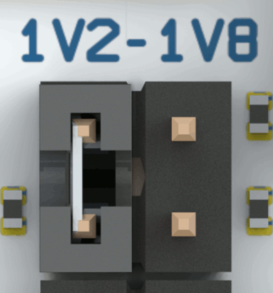 |
If none of the described voltage levels is suitable for the used camera: you can configure custom voltages in the range from 1.2 V to 3.3 V by using resistors instead of jumpers for connecting the pins. The output voltage can be determined by formula (1).
- \(R\) is the resistance that results from the applied circuit (see equation (2))
- \(R_{left}\) is the resistance of the left jumper replacement
- \(R_{right}\) is the resistance of the right jumper replacement
The following figure shows the circuit. Pin header 1V2-1V8 is called X8 in the circuit diagram. Also illustrated is the relation between the pin header orientation in the schematic and on the board.

2V8-3V3 Pin Header options🔗
| Voltage on 2V8-3V3 (AVDD) | Jumper Configuration |
|---|---|
| 1.87V (unusual) | 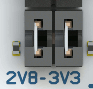 |
| 2.8V | 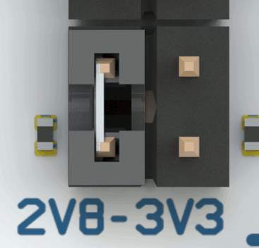 |
| 3.0V | 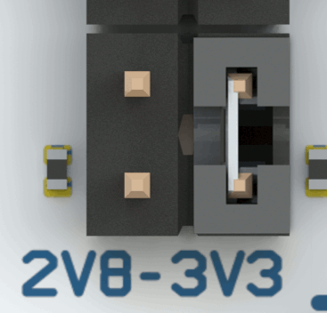 |
| 3.3V |  |
If none of the described voltage levels is suitable for the used camera: you can configure custom voltages in the range from 1.87 V to 3.3 V by using resistors instead of jumpers for connecting the pins. The output voltage can be determined by formula (3).
- \(R\) is the resistance that results from the applied circuit (see equation (4))
- \(R_{left}\) is the resistance of the left jumper replacement
- \(R_{right}\) is the resistance of the right jumper replacement
The following figure shows the circuit. Pin header 2V8-3V3 is called X7 in the circuit diagram. Also illustrated is the relation between the pin header orientation in the schematic and on the board.
PAN9520 RF Switch (SPDT) Control🔗
Beside the usage of the chip antenna, the PAN9520 gives also the option to use a bottom pad to give out the RF signal. For the configuration which option is used an integrated Single Pole Double Throw (SPDT) RF switch is used.
The bottom pad is connected to the U.FL connector RF of the evaluation board. You can access the SPDT control lines via the SPDT control pin header 20.
Valid configurations🔗
Note
Please note that other configurations (than those that are shown below) lead to unspecified states of the SPDT RF switch.
| Configuration Description | Jumper Configuration on SPDT Ctrl |
|---|---|
| The on-board chip antenna is used |  |
| Module's on-board chip antenna is used (configured by on-board pull-resistors) | |
| U.FL connector "RF" is used |  |
Interface Pin Assignment Overview🔗
The following table gives you a quick overview of the GPIOs and the interfaces they are used for. Please note that all GPIOs are additionally connected to the GPIO breakout headers.
| Pin | LEDs | Buttons | UART0 | Camera Interface | Arduino Interface | JTAG | USB |
|---|---|---|---|---|---|---|---|
| GPIO0 | SW1/IO0 | Evaluated at start-up (strapping pin) | |||||
| GPIO1 | SW2 | A0 | |||||
| GPIO2 | SW3 | A1 | |||||
| GPIO3 | SW4 | VSYNC | A2 | ||||
| GPIO4 | PWDN | A3 | |||||
| GPIO5 | HREF | A4 | |||||
| GPIO6 | D9 | A5 | |||||
| GPIO7 | SIOC | I²C SCL | |||||
| GPIO8 | SIOD | I²C SDA | |||||
| GPIO9 | D9 | ||||||
| GPIO10 | XCLK | D8 | |||||
| GPIO11 | D8 | D7 | |||||
| GPIO12 | D7 | D6 | |||||
| GPIO13 | PCLK | D5 | |||||
| GPIO14 | D6 | D4 | |||||
| XTAL_32K_P (GPIO15) | D2 | D3 | |||||
| XTAL_32K_N (GPIO16) | D5 | D2 | |||||
| DAC_1 (GPIO17) | D3 | D1 U1RX/TX | |||||
| DAC_2 (GPIO18) | D4 | D0 U1TX/RX | |||||
| GPIO19 | USB D- | ||||||
| GPIO20 | USB D+ | ||||||
| GPIO21 | LED1 | ||||||
| GPIO33 | LED2 | ||||||
| GPIO34 | D10 (SS) | ||||||
| GPIO35 | D11 (MOSI) | ||||||
| GPIO36 | D13 (SCK) | ||||||
| GPIO37 | D12 (MISO) | ||||||
| GPIO38 | LED3 | ||||||
| MTCK (GPIO39) | MTCK | ||||||
| MTDO (GPIO40) | MTDO | ||||||
| MTDI (GPIO41) | MTDI | ||||||
| MTMS (GPIO42) | MTMS | ||||||
| U0TXD (GPIO43) | U0TXD | ||||||
| U0RXD (GPIO44) | U0RXD | ||||||
| GPIO45 | Evaluated at start-up (strapping pin) | ||||||
| GPIO46 | Evaluated at start-up (strapping pin) | ||||||