User Guide🔗
Introduction🔗
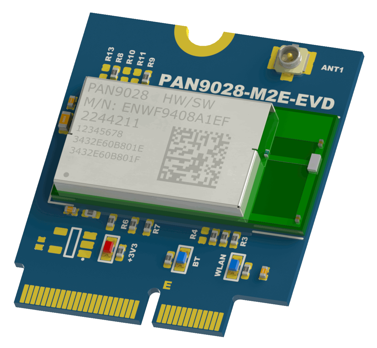
The PAN9028 M.2 device (ENWF9408AMEF) is an evaluation device (EVD) ideally suited for use of the module in conjunction with host processor evaluation kits that have a M.2 Key E socket.
It features a PAN9028 with an integrated Power Management IC (ENWF9408A1EF).
Features🔗
- M.2 Key E form factor
- External antenna U.FL connector
- Coexistence interface
- Wi-Fi and Bluetooth status indicator LEDs
- PCM interface
Block Diagram🔗

Board Overview🔗

1
The module
2
Mounting screw indentation
You can use the mounting screw indentation to secure the board in a M.2 Key E socket. Also see Mounting the Device
3
External antenna U.FL connector - ANT1
You can use the U.FL connector to connect an external antenna. Also see Antenna Configuration
4
Wi-Fi status indicator LED
The Wi-Fi status indicator LED for indicating the Wi-Fi status is currently non-operational.
5
Bluetooth status indicator LED
The Bluetooth status indicator LED for indicating the Bluetooth status is currently non-operational.
6
M.2 Key E connector
You can insert the PAN9028 M.2 device into a M.2 Key E socket to connect the modules interfaces to a host processor. Also see M.2 Connector Pin Map
7
Power LED
You can observe the power LED to verify that the board is correctly powered.
Device Dimensions🔗

Initial Preparations🔗
Mounting the Device🔗
To mount the PAN9028 M.2 device in a M.2 Key E socket on a host board execute the following instructions.
-
Line up the notch on the M.2 Key E connector 6 with the key of the M.2 Key E socket of the host board.
-
Insert the PAN9028 M.2 device into the socket slightly angled.

-
Apply some light downward pressure until the PAN9028 M.2 device is parallel to the host board and makes contact to the threaded insert.

-
Insert a M2.5 x 4 machine screw into the mounting screw indentation 2 and the threaded insert.

The PAN9028 M.2 device is secured in place.
M.2 Connector Pin Map🔗
| Description | M.2 Key E Pin | Function | Module Footprint | Module Pin |
|---|---|---|---|---|
| SDIO Interface | 9 | SDIO CLK | G5 | SD_CLK |
| 11 | SDIO CMD | G6 | SD_CMD | |
| 13 | SDIO DATA0 | G7 | SD_DAT0 | |
| 15 | SDIO DATA1 | G8 | SD_DAT1 | |
| 17 | SDIO DATA2 | G9 | SD_DAT2 | |
| 19 | SDIO DATA3 | G10 | SD_DAT3 | |
| UART Interface | 22 | UART RXD / GPIO8 | B8 | UART_SOUT / IO8 |
| 32 | UART TXD / GPIO9 | A8 | UART_SIN / IO9 | |
| 34 | UART RTS / GPIO11 | A7 | UART_RTS / IO11 | |
| 36 | UART CTS / GPIO10 | B8 | UART_CTS / IO10 | |
| Status LEDs | 6 | Wi-Fi LED / GPIO2 | F8 | LED_WLAN / IO2 |
| 16 | Bluetooth LED / GPIO3 | F9 | LED_BT / IO3 | |
| PCM Interface | 8 | I2S SCK / GPIO6 | E1 | PCM_CLK / IO6 |
| 10 | I2S WS / GPIO7 | F6 | PCM_SYNC / IO7 | |
| 12 | I2S SD IN / GPIO5 | F7 | PCM_DOUT / IO5 | |
| 14 | I2S SD OUT / GPIO4 | F10 | PCM_DIN / IO4 | |
| Coexistence Interface |
46 | Coexistence RXD / GPIO17 | B10 | COEX_OUT / IO17 |
| 48 | Coexistence TXD / GPIO16 | F5 | COEX_SIN / IO16 | |
| Clock | 50 | 32 KHz Oscillator | E6 | 32KHZ_IN |
| Power | 2, 4, 72, 74 | 3.3 V | F2, F3 | VDD3V3 |
| 56 | PMIC Enable | A2 | PMIC_EN | |
| 1, 7, 18, 33, 39, 45, 57, 63, 69, 75 |
GND | A1, A12, B12, C11, C12, D11, D12, E11, E12, F1, F11, F12, G11, EP1, EP2, EP3, EP4 |
GND, EPAD1, EPAD2, EPAD3, EPAD4 |
|
| not connected | 3, 5, 7, 20, 21, 23, 35, 37, 38, 40, 41, 42, 43, 44, 47, 49, 52, 53, 54, 55, 58, 59, 60, 61, 62, 64, 65, 66, 67, 68, 70, 71, 73 |
not connected | N/A | N/A |
Clock Configuration Pin
The UART_SOUT (M.2 Key E pin 22) doubles as a configuration pin for the clock frequency used by the PAN9028.
Only the 26 MHz configuration is valid since the PAN9028 includes a crystal with this frequency.
Keep this pin floating or on logical high level during firmware initialization. A low level during firmware initialization prevents the firmware from starting up.
Hardware Modifications🔗
You can modify the PAN9028 M.2 device to suit your application and your specific host processor by making some hardware modifications.
The following sections describe how you can reconfigure the reference voltages and how you activate the external antenna U.FL connector ANT1 3.
SDIO Reference Voltage🔗
In case your host processor board only supports a SDIO signal voltage of 3.3 V you can reconfigure the PAN9028 M.2 device to use the 3.3 V generated by the PMIC as VIOSD.
The PAN9028 supports 1-bit or 4-bit SDIO transfer modes with full clock range up to 208 MHz. The SDIO interface pins are powered from the VIOSD voltage supply with either 1.8 V or 3.3 V.
On the PAN9028 M.2 device by default VIOSD is connected to the VOUT1V8 of the PMIC, hence it is set to 1.8 V.
IO Reference Voltage
Setting VIOSD to 3.3 V also configures the IO reference voltage to be 3.3 V as well.
To set VIOSD to 3.3 V execute the following instructions.
-
Unsolder the resistors R8 and R9.
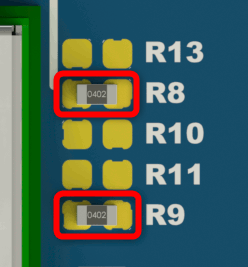
-
Place a 0 Ohm resistor (0402) for R13 and or bridge it with a solder blob.

-
Place a 0 Ohm resistor (0402) for R10 and or bridge it with a solder blob.
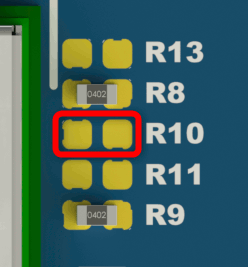
This connects VIOSD to 3.3 V.
Note
SDIO clock speeds higher than 50 MHz can only be achieved with a SDIO signal voltage level (VIOSD) of 1.8 V and a host processor that supports the SDIO 3.0 Standard.
The maximum achievable data rate is limited by the used SDIO clock speed.
For further information please refer to the module product specification at
IO Reference Voltage🔗
In case your host processor board supports only IO voltage levels of 3.3 V you can reconfigure the PAN9028 M.2 device to use 3.3 V as voltage level for its UART and IOs.
The voltage used by the IOs and the UART interface is determined by the voltage applied to VIO. You can configure it to either 1.8 V or 3.3 V.
On the PAN9028 M.2 device by default VIO is connected to VOUT1V8 of the PMIC, hence it is set to 1.8 V.
Warning
In case you have set VIOSD to 3.3 V as described in SDIO Reference Voltage the IO reference voltage is also configured to be 3.3 V.
Please note, if VIOSD is set to 3.3 V it is not possible to set the IO reference voltage to 1.8 V since this would create a short between 3.3 V and 1.8 V.
To set VIO to 3.3 V execute the following instructions.
-
Unsolder R8.
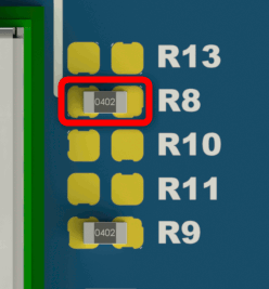
-
Place a 0 Ohm resistor (0402) for R13 or bridge it with a solder blob.
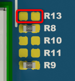
This connects VIO to 3.3 V.
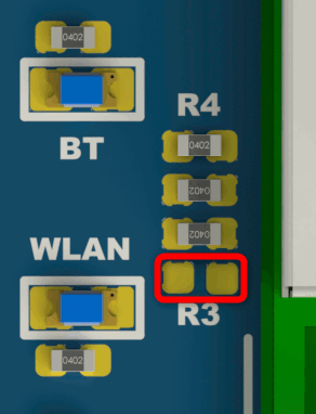
Antenna Configuration🔗
You can evaluate PAN9028 M.2 device in conjunction with an external antenna by activating the external antenna U.FL connector ANT1 3 with some hardware modifications. By default the chip antenna is active.
External Antenna
To activate the external antenna U.FL connector ANT1 3 execute the following instructions.
-
Unsolder R3.
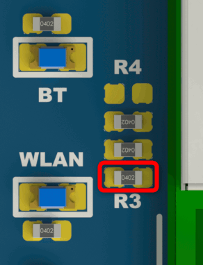
-
Place a 0 Ohm resistor (0402) for R4 or bridge it with a solder blob.
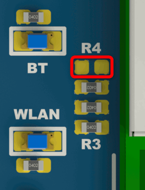
Chip Antenna
In case you modified the PAN9028 M.2 device to use the external antenna U.FL connector ANT1 3 execute the following instructions to switch back to the chip antenna.
-
Unsolder R4.
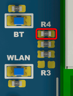
-
Place a 0 Ohm resistor (0402) for R3 or bridge it with a solder blob.